|
 | | Introduction
Being discussed here is my method for making prototype hobby PCBs. It's something I always wanted to do, and tried about 5-years ago with a laundry pen from WH-Smith and ferric cloride. The results were electrically sound let's just say, but not pretty or precise. What you read here is how I've recently set myself up. I am not experienced by any means but I do follow instructions.
Clicking on some of the images here will open them up full size in a new window. |
|
|
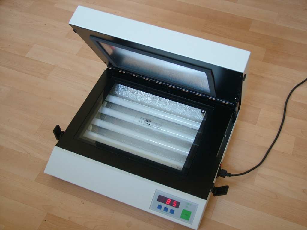
Mega-UK AZ210 Double Sided Vaccuum UV Exposure Box
This device is expensive! They retail for about Ł650+VAT. I bought this recently 2nd hand. It has eight UV tubes, four in the bottom and four in the top. The exposure area is 260 x 355 (10.2" x 14"). When used with Rapid Fotoboard 2 (34-0105) treated PCBs the exposure time is 85-seconds. When exposed the boards have a very feint yellow hue visible. | | 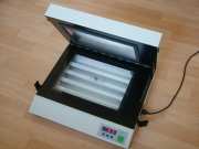 |
|
|
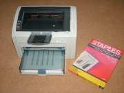 | | HP LaserJet 1022 and Staples SL5041 Transparency Film
I took a bit of a chance with this one, as inkjets have supposedly overtaken lasers for use with PCB development, I just didn't fancy spending Ł6 on 10-sheets of inkjet transfer film and opening up a host of maybe what ifs. The Laserjet 1022 achieves 1200dpi and DOES NOT overheat the transparencies. The printer has a very neat footprint and is insanely fast. |
|
|
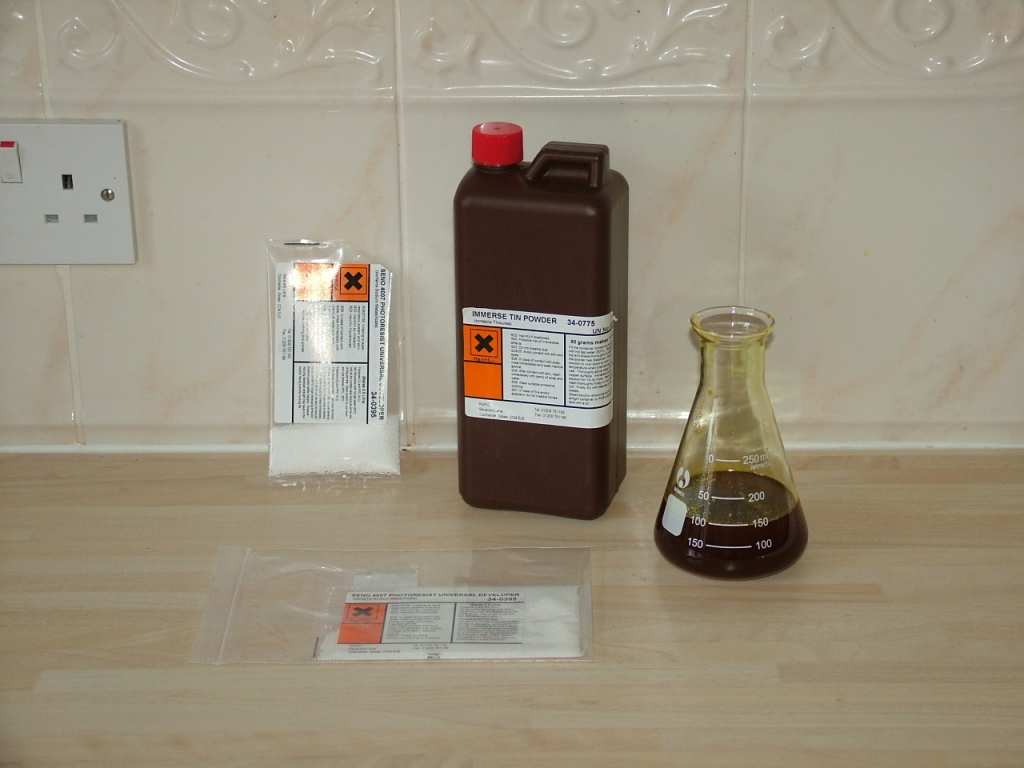
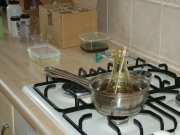
Ferric Cloride, Developer Crystals, Tin Plating Solution
All from Rapid. Ferric cloride (34-0390) in granular form costing Ł3.70. Developer crystals (34-0395) costing Ł0.79. Tin plating solution (34-0775) costing Ł12.65. All of these chemicals are bloody horrible! Make no mistake. | |  |
|
|
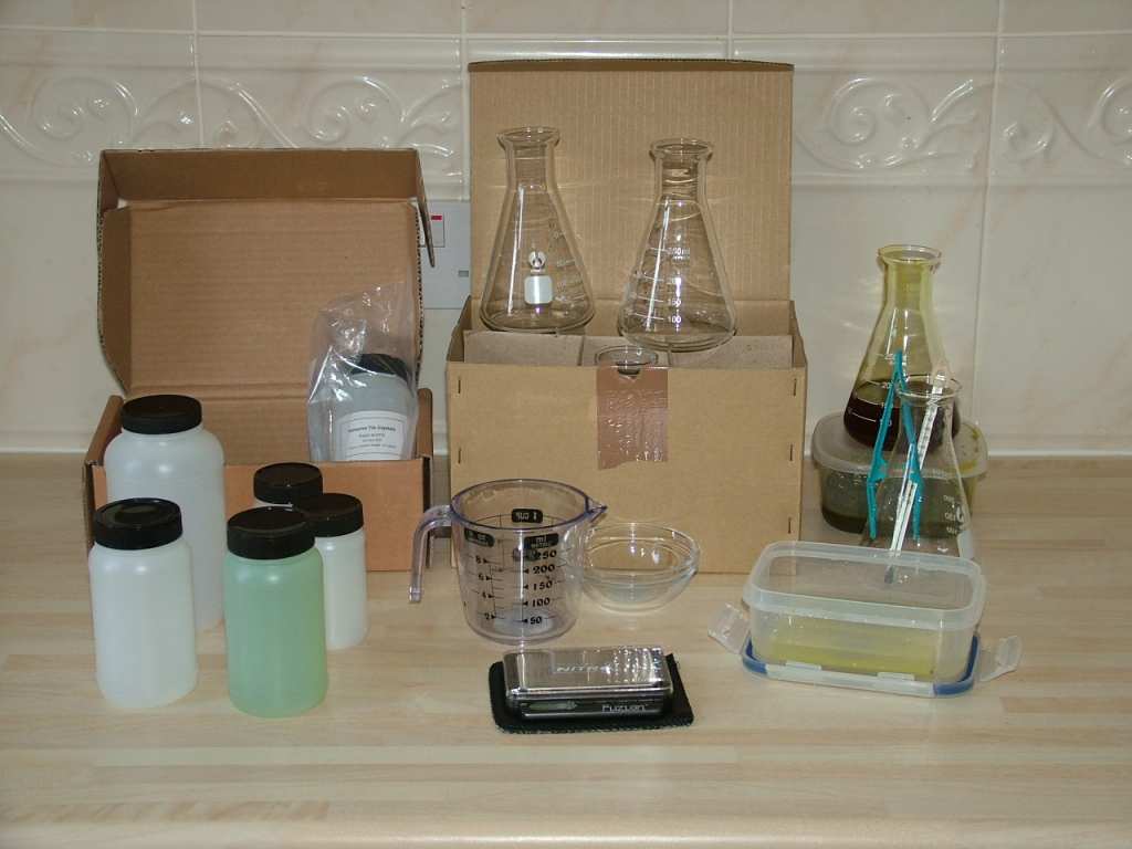
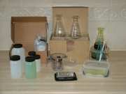 | | PVC Containers, Glass Flasks, Thermometer, Scales
A sensible precaution. I am mixing up only what I need, usually in quantities of 125-250ml. A box of glass flasks is good since you can just grab one without fiddling about. The scales are precise to 0.1g and far more suitable than guessing with kitchen scales especially when the tin plating solution is so expensive. All solutions are also mixed up at the right temperatures. |
|
|
Cadsoft Eagle PCB Design Package
Somehow I just find Eagle to be the standard. I've done this before in the past, where you get to know one package and no one uses it! I am running the freeware edition to be used for non profit projects, which has a board area restriction of 100 x 80mm (4 x 3.2"). Most if not all that I do here is just on a hobbyist basis.
Clicking on the image will take you to the Eagle website. The package is stable and widely recognised. I've been through all of them. | | 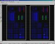 |
|
|
 | | Write Up and My Ramblings
1 mil = 1/1000th of an inch. 50 mil = 0.05" tracks, 10 mil = 0.01" tracks. Normal minimum line width of 12.5 mil = 0.0125" track width. |
|
|
Stage 1
Finalise your design within Eagle, print dozens of copies off on plain paper or however you get there. Print off the final design onto a transparency sheet, and you're ready to go. | | 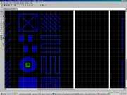 |
|
|
 | | Stage 2
Get all of your nasty chemicals ready and prepared. Have the photo developer ready. Have the ferric cloride ready. Clean out the sink and tidy up. Have EVERYTHING prepared. The developer needs to be at 20-25'C. The ferric cloride needs to be at about 35-50'C. Too cold and it takes ages. Too hot and it gets really aggressive. Fast etching does produce better edge quality and consistent line widths. |
|
|
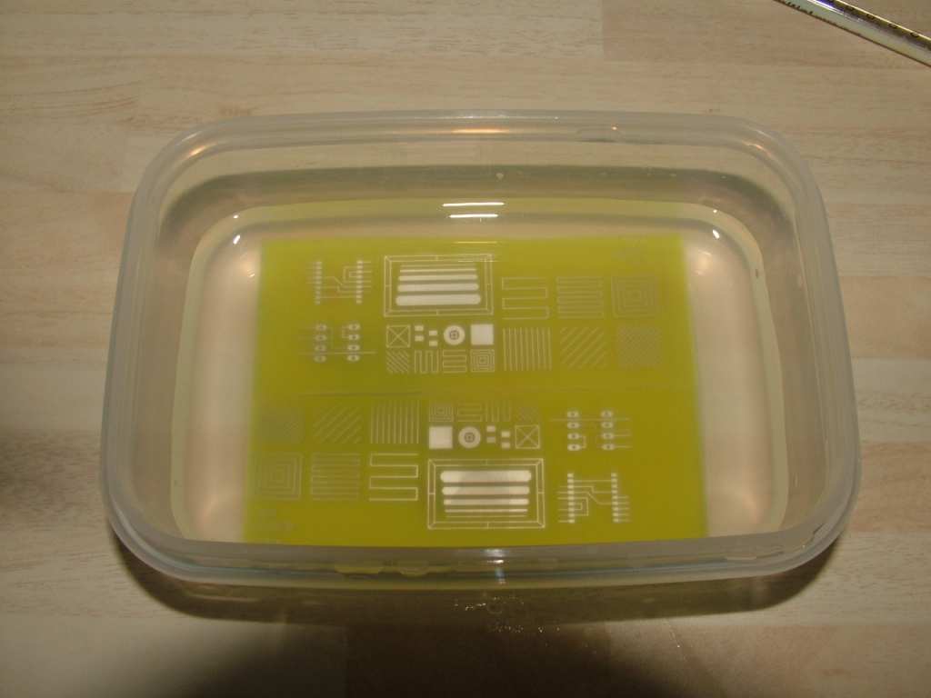
Stage 3
Warm up the UV tubes for 300 seconds. Place the photo sensitive board (with the plastic removed!) face up on the glass. Place the transparent sheet over the top of the black PCB. Turn on the tubes for 85 seconds. Over exposure is better than under exposure. | | 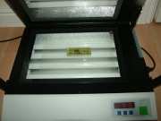 |
|
|
 | | Stage 4
Place the board into the developer for 30-35 seconds, rock back and forth to agitate. Under-exposure is worse than over-exposure. The circuit will appear on the PCB as if by magic. Afterwards clean the PCB in the sink, light water will do. Don't get this stuff in your eyes! Really, else you'll be getting a half price television licence. The unwanted photo resist will gradually waft away and you'll be able to see it doing so. |
|
|
Stage 5
Into the ferric cloride it goes. It doesn't bubble or anything like that, it just sits there. Slowly agitate back and forth. After a few minutes the copper will start to be eaten away from the edges. After a few more minutes you'll end up with one last bit while wondering if the rest of your circuit is going to be eaten away. Agitate throughout. When finished it's time to put the board under the tap again and rinse it. | |  |
|
|
 | | Stage 6
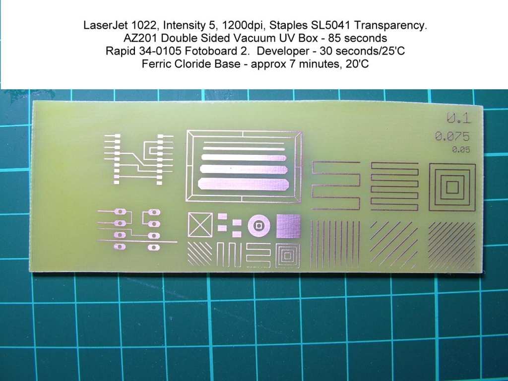
Admire your handywork, show it to other people while they take little if any interest at all. If you so wish you may do another board and not show other people. The thinnest traces on this board are 0.003" or 3 mils. The majority of traces are 0.01" or 10 mils. This board was my very first attempt. |
|
|
Stage 7
The photo resist can be removed with acetone, or in other words, with nail varnish remover. It comes off quite easily. The copper board can then be lightly buffed to remove any remaining resist or residues. This one has been under a scanner at 600dpi. It is better than the previous attempt. The ferric cloride was hotter with this one at about 50'C when it left the stove. | |  |
|
|
 | | Stage 8
Now if you're really determined and having a good time you can now tin plate the board. This takes about 30-minutes to 2-hours depending on how thick you wish to go. Instructions will be provided with whatever you are using. While the board is tinning away go off and set your mind to something else, I'm doing this web page. The photograph you see is after about 30-minutes in the solution. |
|
|